
Die-level reverse engineering
DMG-CPU Research
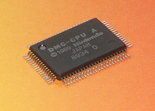
The DMG-CPU is the system-on-a-chip of the original Nintendo Game Boy. This project rebuilds it from silicon: modules are traced from die photographs with the Deroute utility into netlists and die-perfect Verilog — and the real netlists are exercised by Icarus regression suites for the SM83 core, PPU, APU and the small clock/arbiter/MMIO/serial domain.
- die-perfect Verilog netlist
- Icarus regression suites on the real netlist
- open research, sources in the repo
§1 The SoC
functional blocks of the LR35902 system-on-a-chipSoC overview
Block diagram, architecture notes and the full internal bus list of the chip.
1.02Bonding pads & I/O terminals
Pinout and pad circuits of the DMG-CPU.
1.03Cells library
The standard cells the SoC is built from.
1.04Clock generator
The bushy clock tree that drives the whole chip.
1.05Serial link
Serial I/O (link port) circuitry.
1.06Bus arbiter
Arbitration between internal and external buses.
1.07MMIO & interrupts
Divider, timer, DMA and the interrupt controller (IF).
1.08HRAM
The internal high RAM macro.
1.09Boot ROM
The mask-ROM holding the bootstrap program.
1.10OAM
The object-attribute memory macro.
1.11PPU
Picture processing unit index; PPU1 + PPU2 split and links.
1.12PPU1 — BG/WIN
Background & window pipeline, H/V counters, LCD interface.
1.13PPU2 — sprites
Object / OAM side of the pipeline.
1.14APU — sound
Four-channel sound generator (chips-era synthesis).
1.15Wave RAM
The channel-3 sample RAM macro.
1.16Sound DAC
The audio output digital-to-analogue stage.
1.17Schematics
Module circuits compared against @msinger's dmg-schematics.
1.18@msinger's map
Cell-by-cell rows of the Rev B die map.
§2 SM83 core
the Game Boy CPU: topology, buses, ALU, decoders, sequencerCore overview
Component map of the core; where every block sits on the die.
2.02Topology
Metal/poly/diffusion layers and how the core is organised.
2.03Buses
Internal data movement: rbus, wbus, idu, hl bus.
2.04Rails & precharge
Power rails and the old-school bus-precharge trick.
2.05Clocks
The clock set the core consumes.
2.06Ports
Core I/O against the rest of the SoC.
2.07Register file
Registers, SP, PC and the incrementer/decrementer.
2.08ALU & flags
The arithmetic/logic unit and the Z/N/H/C flag block.
2.09Data mux
Bus multiplexing and the datalatch.
2.10IDU
The instruction decoder units.
2.11Sequencer
The M/T-cycle state machine that drives everything.
2.12Decoder 1
First-level instruction decoder output table.
2.13Decoder 2
Second-level decoder output table.
2.14Decoder 3
Third-level decoder: the w/x signal law.
2.15The Thingy
The small but important circuit next to the decoder.
2.16Interrupts
IRQ control logic of the core.
2.17Investigations
Historical debug notes from bringing up the SM83 HDL.
2.18SM83 reference
Opcode tables and external references.
§3 Verilog & regression suites
die-perfect HDL driven by Icarus testbenchesSM83 core HDL
All core modules as Verilog.
3.02Icarus suites & tooling
Regression suites and the GTKWave-based workflow.
3.03SM83 suite
Icarus regression on the real SM83 netlist (issue #400).
3.04SM83 suite — waves
Waveform documentation of every suite test.
3.05SM83 suite — status
Per-test status and measured timing facts.
3.06Small-domain suite
ClkGen / Arb / MMIO / Ser testbench (issue #396).
3.07Small-domain — waves
Waveform documentation: mmio, ser, hram, arb, clkgen, div.
3.08PPU suite
PPU1/PPU2 testbench (issue #390).
3.09PPU suite — waves
Waveform documentation: regs, frame, scroll, window, sprites.
3.10APU suite
APU testbench (issue #398).
3.11APU suite — waves
Waveform documentation: channels 1–4, mix, regs.
3.12GTKWave skill
How the waves are rendered (vcd2png + .gtkw).
§4 References & process
how the research is done and where the data livesReference PCB
DMG-CPU-06 board reconstruction used for verification.
4.02Research methods
ACID-FREE chip opening and imaging workflow.
4.03Datasets
Public die photographs per chip revision.
4.04Netlists
Recovered netlists and the Deroute workflow.
4.05SM83 netlist
Core netlist sources.
4.06SoC netlist
Rest-of-chip netlist sources.
4.07Logisim models
Interactive models of the most intricate circuits.
4.08Layer imagery
SM83 core topography pictures: metal, poly, diffusion, vias.
4.09BANK register
The $FF50 BANK register circuit.