This is where the functional simulators of large chips and cores are located.
M6502Core
MOS 6502 processor core emulator on the gate level.
Yeah, it's that simple. We take the 6502 logic circuits from Wiki and just duplicate them in C++.
To understand what's going on here, it's enough to understand how circuits work. The code simply repeats their work.
Approaches to simulation
Some modules are simulated immediately with output values. And for some, simulation and output values are separated for convenience.
In general, the source code is a bit like Verilog, but unlike the latter, we choose the sequence of execution of circuit elements ourselves, thereby imitating the propagation delay that we have in real circuits.
If the module has few inputs/outputs, they are passed as parameters. If there are a lot of inputs/outputs, an array indexed by enum definitions is used as a parameter.
Combinatorial and sequential circuits
As you know, there are two types of circuits: simple unidirectional gate cascades (NOR, NAND) and cyclic (sequential) Flip/flops circuits.
Combinatorial circuits are simulated simply by repeating the operation of the gates. No gimmicks.
The following approach is applied to sequential circuits (FF's):
- The input stage uses the stored FF value (
ff.get) - The output stage updates the current FF value (
ff.set) - This makes no difference between which elements the FF is based on. It can be 2 closed inverters, 2 closed NOR or any other cyclic closure
- The "storage" location of FF on the cyclic circuit is chosen arbitrarily, but usually closer to the FF output
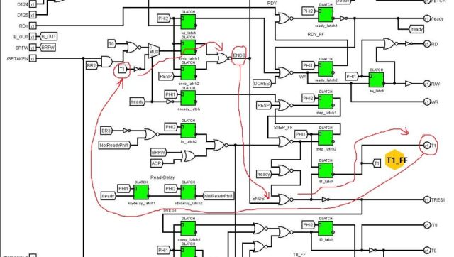
It should be noted that the 6502 has quite a few hidden and quite twisted loops, for example:
Buses
Modules connected to internal buses require a special approach and a certain order of execution, as written here: https://github.com/emu-russia/breaks/blob/master/BreakingNESWiki_DeepL/6502/context_control.md
You should also consider the case when several sources (e.g. registers) put their values on the same bus at the same time. To solve such situations ("bus conflicts") it is necessary to use the "Ground wins" rule.
This takes into account the 6502 feature where buses are "precharged" during PHI2. This is required to form constants (e.g. stack address, interrupt address). Charging is done at the very beginning of the simulation.
Optimization
The M6502Core can, with some stretch, be called suitable for real-time applications.
The following approaches are used for optimization:
- Separation of PHI1/PHI2 phases by if/else
- Precomputing combinatorial logic with tables (see e.g. predecode.cpp).
- Packing of bus and register bits into uint8_t, avoids for loops on all bits
- High level logic circuits simulation (see e.g. alu.cpp).
The bottleneck is random logic, which consumes 50-60% of computing time.
Besides, now both parts are simulated 2 times every half cycle, to stabilize latches.
APUSim
APU simulator at the gate level.
Note: In the Breaks project, the term APU refers to the entire CPU chip (2A03/2A07), which includes the 6502 core and the APU itself. Therefore, here APU and CPU are synonymous.
Simulation Approaches
In general, all approaches are tried on the M6502Core, in terms of APU nothing particularly new. We take the circuit and repeat its work in C++. In the beginning somehow, and then we try to optimize it.
All of the APU schematics can be found here: https://github.com/emu-russia/breaks/tree/master/BreakingNESWiki_DeepL/APU
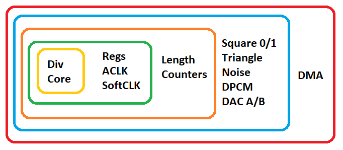
To simplify understanding, the following image shows the "layers" in which the individual parts of the APU are simulated:
PPUSim
PPU simulator at the gate level.
Simulation Approaches
In general, all approaches are tried on the M6502Core, in terms of PPU nothing particularly new. We take the circuit and repeat its work in C++. In the beginning somehow, and then we try to optimize it.
All of the PPU schematics can be found here: https://github.com/emu-russia/breaks/tree/master/BreakingNESWiki_DeepL/PPU
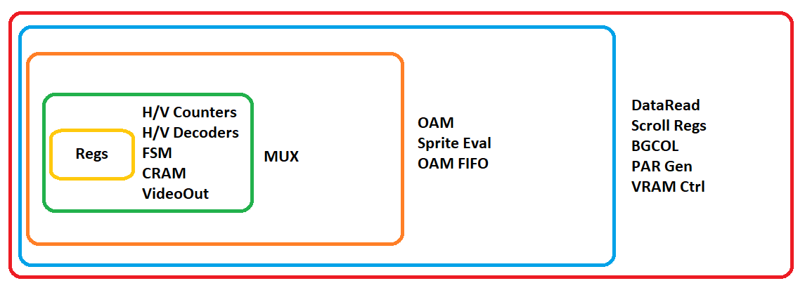
To simplify understanding, the following image shows the "layers" in which the individual parts of the PPU are simulated: